ISC Physics 2021 Specimen Paper for Class-12 Solved Question Paper for practice. Step by step Solutions with section-A, B, C and D. Visit official website CISCE for detail information about ISC Class-12 Physics.
By the practice of ISC Physics 2021 Specimen Paper for Class-12 Solved Previous Year Question Paper you can get the idea of solving. Try Also other year except ISC Physics 2021 Specimen Paper for Class-12 Solved Question Paper of Previous Year for more practice. Because only ISC Physics 2021 Specimen Paper for Class-12 is not enough for complete preparation of next council exam.
ISC Physics 2021 Specimen Paper for Class-12 Solved
-: Included Topics :-
Section-A
Section-B
Section-C
Section-D
ISC Physics 2021 Specimen Paper for Class-12 Solved
Maximum Marks: 70
Time allowed: Three hours
- Candidates are allowed additional 15 minutes for only reading the paper. They must NOT start writing during this time.
All questions are compulsory. - This question paper is divided into 4 Sections, A, B, C and D as follows :
- Section A: Question number 1 is of twelve marks. All parts of this question are compulsory.
- Section B: Question numbers 2 to 12 carry 2 marks each with two questions having internal choice.
- Section C: Question numbers 13 to 19 carry 3 marks each with two questions having internal choice.
- Section D: Question numbers 20 to 22 are long-answer type questions and carry 5 marks each.
- Each question has an internal choice.
- The intended marks for questions are given in brackets [ ].
- All working, including rough work, should be done on the same sheet as and adjacent to the rest of the answer.
- Answers to sub parts of the same question must be given in one place only.
- A list of useful physical constants is given at the end of this paper.
- A simple scientific calculator without a programmable memory may be used for calculations
Section – A
ISC Physics 2021 Specimen Paper for Class-12 Solved
Question 1.
(a) Choose the correct alternative (a), (b), (c) or (d) for each of the questions given below: [5]
(i) The electrostatic potential energy of two point charges, 1 μC each, placed 1 metre apart in air is :
(a) 9 x 10³ J
(b) P x 109 J
(c) 9 x 10⁻³J
(d) 9 x 10⁻³ eV
(ii) A wire of resistance R ’ is cut into ‘n ’ equal parts. These parts are then connected in parallel with each other. The equivalent resistance of the combination is :
(a) nR
(b) R/n
(c) n/R2
(d) R/n2
(iii) When a light wave travels from air to glass :
(a) its wavelength decreases
(b) its wavelength increases
(c) there is no change in wavelength
(d) its frequency decreases.
(iv) The equivalent resistance between points a and f of the network shown in figure is :
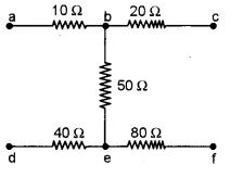


(a) 24 Ω
(b) 110 Ω
(c) 140 Ω
(d) 200 Ω
(v) If Ep and Ek represent potential energy and kinetic energy respectively, of an orbital electron, then, according to Bohr’s theory :
(a) Ek = – Ep/2
(b) Ek = – Ep
(c) Ek= – 2Ep
(d) Ek = 2Ep
(vi) A beam of light is incident at the polarizing angle of 35° on a certain glass plate. The refractive index of the glass plate is :
(a) sin 35°
(b) tan 35°
(c) tan 55°
(d) sin 55°
(vii) In a gamma ray emission from nucleus :
(a) only the number of protons change.
(b) the number of protons and neutrons, both change.
(c) there is no change in the number of protons and the number of neutrons.
(d) only the number of neutrons change
Section – B
ISC Physics 2021 Specimen Paper for Class-12 Solved
Question 2.
A rectangular loop of area 5 mH. has 50 turns and carries a current of 1 A. It is held in a uniform magnetic field of 0. IT, at an angle of 30°. Calculate the torque experienced by the coil.
Question 3.
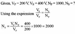
A transformer is used to step up an alternating emf of 200 V to 440 V. If the primary coil has 1000 turns, calculate the number of turns in the secondary coil.
Question 4.
The deviation produced for violet, yellow and red lights for crown glass are 3.75°. 3.25° and 2.86° respectively. Calculate the dispersive power of the crown glass.
Question 5.
Define frequency modulation and state any one advantage of frequency modulation (FM) over amplitude modulation (AM).
Question 6.
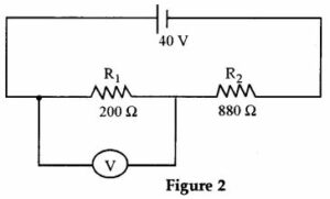
(a) Figure 2 below shows two resistors R1 and R2 connected to a battery having an emf of 40 V and negligible internal resistance. A voltmeter having a resistance of 300 Ω is used to measure potential difference across R1. Find the reading of the voltmeter.
(b) A moving coil galvanometer has a coil of resistance 59 Ω. It shows a full scale deflection for a current of 50 mA. How will you convert it to an ammeter having a range of 0 to 3A ?
Question 7.
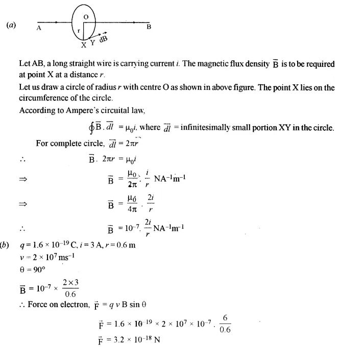
(a) Using Ampere’s circuital law, obtain an expression for the magnetic flux density ‘B’ at a point X’at a perpendicular distance ‘r from a long current carrying conductor. (Statement of the law is not required). [3]
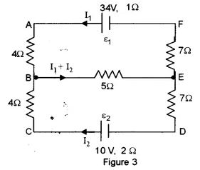
(b) PQ is a long straight conductor carrying a current of 3A as shown in Figure 4 below. An electron moves with a velocity of 2 × 10⁷ ms-1 parallel to it. Find the force acting on the electron.
Question 8.
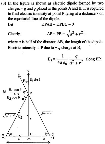
(a) Derive an expression for intensity of electric field at a point in broadside position or on an equatorial line of an electric dipole.
(b) Two point charges of 10 C each are kept at a distance of 3 m in vacuum. Calculate their electrostatic potential energy.
Question 9.
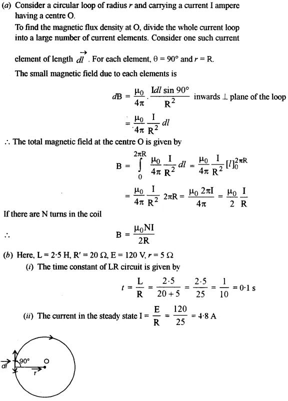
(a) Obtain an expression for magnetic flux density B at the center of a circular coil of radius R, having N turns and carrying a current I. [3]
(b) A coil of self inductance 2.5 H and resistance 20 Ω is connected to a battery of emf 120 V having internal resistance of 5 Ω. Find : [2]
(i) The time constant of the circuit.
(ii) The current in the circuit in steady state.
Question 10.
(i) State de Broglie hypothesis.
(ii) With reference to photoelectric effect, define threshold wavelength.
Question 11.
(a) What is meant by pair annihilation ? Write a balanced equation for the same.
Or
(b) What is meant by the terms half-life of a radioactive substance and binding energy of a nucleus ?
Question 12.
In a communication system, what is meant by modulation? State any two types of modulation.
Section–C
Answer all questions.
ISC Physics 2021 Specimen Paper for Class-12 Solved
Question 13.
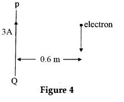
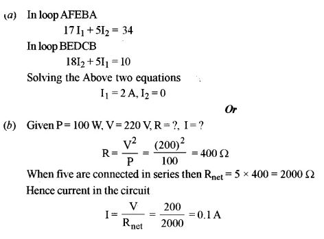
(a) ∈1 and ∈2 are two batteries having emf of 34 V and 10 V respectively and internal resistance of 1 Ω and 2 Ω respectively. They are connected as shown in Figure 3 below. Using Kirchhoff’s’ Laws of electrical networks, calculate the currents I1 and I2.
(b) An electric bulb is marked 200 V, 100 W. Calculate electrical resistance of its filament. If five such bulbs are connected in series to a 200 V supply, how much current will flow through them ?
Question 14.
With reference to semiconductor devices, define ap-type semiconductor and a led diode. What is the use of a led diode ?
Question 15.
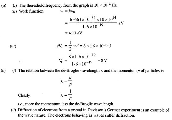
(a) In an experiment of photoelectric effect, the graph of maximum kinetic energy EK of the emitted photoelectrons versus the frequency v of the incident light is a straight line AB as shown in
figure below :
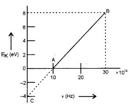
Find :
(i) Threshold frequency of the metal.
(ii) Work function of the metal.
(iii) Stopping potential for the photo electrons emitted by the light of frequency v= 30 × 1014 Hz.
(b)
(i) State how de-Broglie wavelength (λ) of moving particles varies with their linear momentum (p). [2]
(ii) State any one phenomenon in which moving particles exhibts wave nature.
Question 16.
(a) On the basis of Bohr’s theory, derive an expression for the radius of the nth orbit of an electron of hydrogen atom. [3 ]
(b) Using the constants given on end of this Paper, find the minimum wavelength of the emitted X rays, when an X ray tube is operated at 50 kV [2]
Question 17.
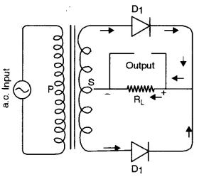
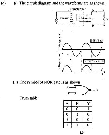
(a) Draw a labelled diagram of a full wave rectifier. Show how output voltage varies with time, if input voltage is a sinusoidal voltage. [3]
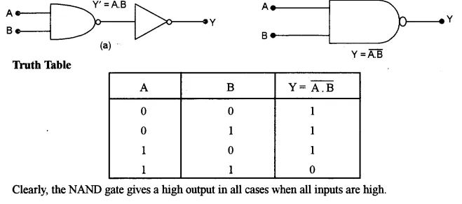
(b) What is a NAND gate ? Write its truth table. [2]
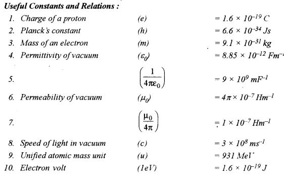
Useful Constants and Relations :
Question 18.
(a) With reference to a semiconductor diode, what is meant by :
(i) Forward bias
(ii) Reverse bias
(iii) Depletion region
(b) Draw a diagram to show how NAND gates can be combined to obtain an OR gate (Truth table is not required). [2]
Question 19.
Derive the law of reflection using Huygens’s Wave Theory.
Section – D
ISC Physics 2021 Specimen Paper for Class-12 Solved
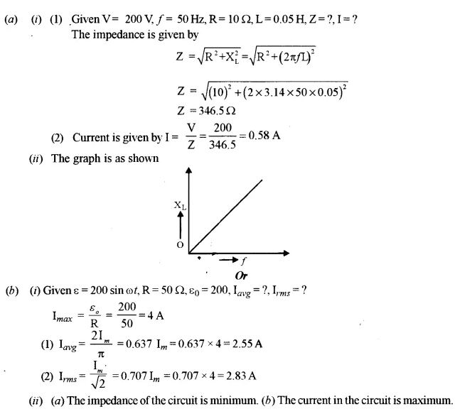
Question 20.
(a) An alternating emf of 200 V, 50 Hz is applied to an L – R circuit, having a resistance R of 10 Ω . and an inductance L of 0.05 H connected in series. Calculate :
(1) Impedance.
(2) Current flowing in the circuit.
(ii) Draw a labelled graph showing the variation of inductive reactance (XL) verses frequency (f).
OR
(i) An a.c. source of emf e = 200 sin ωt is connected to a resistor of 50 Ω
Calculate:
(1) Average current (Iavg).
(2) Root mean square (rms) value of emf.
(ii) State any two characteristics of resonance in an LCR series circuit.
Question 21.
(a)
(i) Draw a labelled circuit diagram of a half wave rectifier and give its output waveform.
(ii) Draw a symbol of NOR gate and write its truth table.
Or
(b)
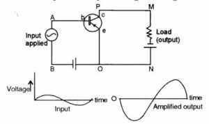
(i) Draw a neat circuit diagram to study the input and output characteristics of a common emitter transistor.
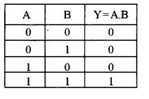
(ii) Draw the symbol for AND gate and write its truth table.
Question 22.
(a) Draw a labelled energy band diagram for a solid which is an insulator. What is the main difference between this diagram and that of a semiconductor ? [3]
(b) Figure below shows the circuit of an electronic device : [3]
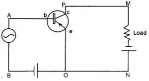
(i) Which electronic device : a rectifier, an amplifier or an oscillator does the above circuit represent ?
(ii) State where the input voltage is applied and where the output voltage is available.
(iii) Compare the output voltage of this circuit with its input voltage.
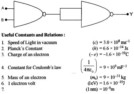
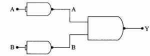
(c) Prepare a truth table for the combination of gates shown in figure below : [2]
-: Solution :-
ISC Physics 2021 Specimen Paper for Class-12 Solved
Answer 1.
(i) (b) P x 109 J
(ii) (b) R/n
(iii) (c) there is no change in wavelength
(iv) (c) 140 Ω
(v) (a) Ek = – Ep/2
(vi) (a) sin 35° and (b) tan 35°
(vii) (a) and (c)
Answer 2.
Given, A= 5 m2, n = 50, I = 1 A, B = 0.1T, θ= 30°, T= T
![]()
Answer 3.
Answer 4.
Given δV = 3.75°, δY = 3.25°, δR = 2.86°
Using the expression for dispersive power ![]()
Answer 5.
When the frequency of the carrier wave changes in accordance with the frequency of the signal it is called frequency modulation. External noise does not have any effect on frequency modulation.
Answer 6.
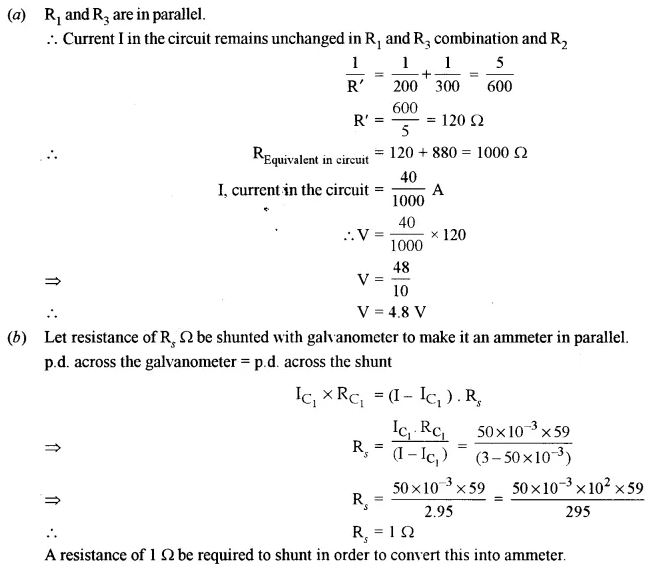
Answer 7.
Answer 8.
(a) In the figure is shown as electric dipole formed by two charges – q and q placed at the points A and B. It is required to find electric intensity at point P lying at a distance r on the equatorial line of the dipole.
Answer 9.
Answer 10.
(i) It states that matter has dual nature.
(ii) It is the wavelength below which photoelectric effect takes place.
Answer 11.
(a) In the pair annihilation, the electron and positron in the stationary state combine with each other and annihilate. Surely, the particles are disappeared and radiation energy will occur instead of two particles.
K– + K+ + 2m0c2 = 2 hv where K– and K+ represent the kinetic energy of the electron and positron before the collision. Also, 2 m0c2 means the rest mass energy of both particles.
Or
(b) Half life: It is the time in which half the nuclei disintegrate.
Binding energy : It is the energy required to disintegrate a nucleus.
Answer 12.
Modulation is the superimposition of a low frequency signal over a high frequency signal.
(i) Amplitude modulation
(ii) Frequency modulation
Answer 13.
Answer 14.
Principle and uses of led
Answer 15.
Answer 16.
(a) Let the electrons of mass m be moving with a velocity vn in an orbit of radius r around the nucleus of hydrogen carrying a charge + e. Since the electrostatic force between the electron and proton supplies the necessary electrostatic force.

Answer 17.
(a) The labelled diagram of a full wave rectifier is given alongside :
D1, D2 are junction diodes. P and S are the primary and secondary of a transformer.
RL = Output resistance across the output is taken. Arrows indicate the direction of current when the diodes are forward biased.
(b) NAND gate : It consists of a combination of AND gate and a NOT gate. The ‘NOT’ negates the output of a NAND gate. It is represented by 
The schematic representation, symbolic representation and its Truth Table are given below:
Answer 18.
(i) Forward bias: When a battery’ is connected to a p-n diode such that the current is in the direction of diode current, the arrangement is called forward bias.
(ii) If the current flows opposite to the direction of diode current, this is called reverse bias.
(iii) Depletion Zone : In p-n diode, the region in which electrons and holes neutralize each other is called depletion region or zone.
Answer 19.
Consider a plane wave front AB incident obliquely on a plane reflecting surface MM’. Let us consider the situation when one end A of wave front strikes the mirror at an angle i but the other end B has still to cover distance BC. Time required for this will be t = BC/ c.
According to Huygens’s principle, point A starts emitting secondary wavelets and in time t, these will cover a distance c,t = BC and spread. Hence, with point A as center and BC as radius, draw a circular arc. Draw tangent CD on this arc from the point C. Obviously. CD is the reflected wave front inclined at an angle r. As incident wave front and reflected wave front both are in the plane of paper, 1st law of reflection is proved.
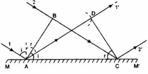
To prove second law of reflection, consider ΔABC and ΔADC. BC = AD (by construction)
∠ABC = ∠ADC = 90° and AC is common. Therefore, the two triangles are congruent and, hence, ∠B AC = ∠DCA or ∠i = ∠r i.e., the angle of reflection is equal to the angle of incidence, which is the second law of reflection.
Answer 20.
Answer 21.
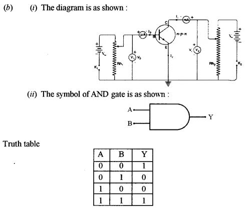
Answer 22.
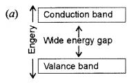
The main difference in energy band diagram of solid insulator and that of conductor is in case of insulator there is wide energy gap between valance band and conduction band whereas this gap is small in case of semiconductor.
(b)
(i) This is the circuit diagram of a common emitter amplifier (using p-n-p transistor)
(ii) The input is applied in between AB and the output is obtained at load i.e., in between MN.
(iii) The output and input voltage of the given circuit has the phase difference of 180° i.e., there is a phase reversal as shown in the diagram alongside.
(c) A study of the gates shows that it is a NAND gate followed by a NOT gate i.e., it represents a AND gate.
Its truth table is as given below:

-: End of ISC Physics 2021 Specimen Paper for Class-12 Solved Question Paper :-
Return to – ISC Class-12 Solved Previous Year Question Paper
Thanks
Please Share with Your Friends