Nootan Solutions Junction Diode ISC Class-12 Physics Ch-32 Nageen Prakashan Numericals. Step by step Solutions of Kumar and Mittal ISC Physics Class-12 Nageen Prakashan Numericals Questions. Visit official Website CISCE for detail information about ISC Board Class-12 Physics.
Nootan Solutions Junction Diode ISC Class-12 Physics Ch-32
| Board | ISC |
| Class | 12 |
| Subject | Physics |
| Publication | Nageen Prakashan |
| Writer | Kumar and Mittal |
| Vol | 2nd |
| Book Name | Nootan |
| Chapter-32 | Junction Diode |
| Topics | Solution of Numericals Questions |
| Page-Number | 1085 |
Nootan Solutions Junction Diode ISC Class-12 Physics Ch-32
P-N Junction :-
A p-n junction is an interface or a boundary between two semiconductor material types, namely the p-type and the n-type, inside a semiconductor.
The p-side or the positive side of the semiconductor has an excess of holes and the n-side or the negative side has an excess of electrons. In a semiconductor, the p-n junction is created by the method of doping. The process of doping is explained in further detail in the next section.
Biasing conditions for the p-n Junction Diode :-
There are two operating regions in the p-n junction diode:
- P-type
- N-type
There are three biasing conditions for p-n junction diode and this is based on the voltage applied:
- Forward bias: The positive terminal of the voltage potential is connected to the p-type while the negative terminal is connected to the n-type.
- Reverse bias: The negative terminal of the voltage potential is connected to the p-type and the positive is connected to the n-type.
- Zero bias: There is no external voltage applied to the p-n junction diode.
Reverse Bias :-
When the p-type is connected to the negative terminal of the battery and the n-type is connected to the positive side then the p-n junction is said to be reverse biased. In this case, the built-in electric field and the applied electric field are in the same direction. When the two fields are added, the resultant electric field is in the same direction as the built-in electric field creating a more resistive, thicker depletion region. The depletion region becomes more resistive and thicker if the applied voltage becomes larger.
current flow in PN junction diode :-
The flow of electrons from the n-side towards the p-side of the junction takes place when there is an increase in the voltage. Similarly, the flow of holes from the p-side towards the n-side of the junction takes place along with the increase in the voltage. This results in the concentration gradient between both sides of the terminals. Due to the formation of the concentration gradient, there will be a flow of charge carriers from higher concentration regions to lower concentration regions. The movement of charge carriers inside the p n junction is the reason behind the current flow in the circuit.
Nootan Numerical Solutions Junction Diode ISC Class-12 Physics Ch-32
Nageen Prakashan Numericals
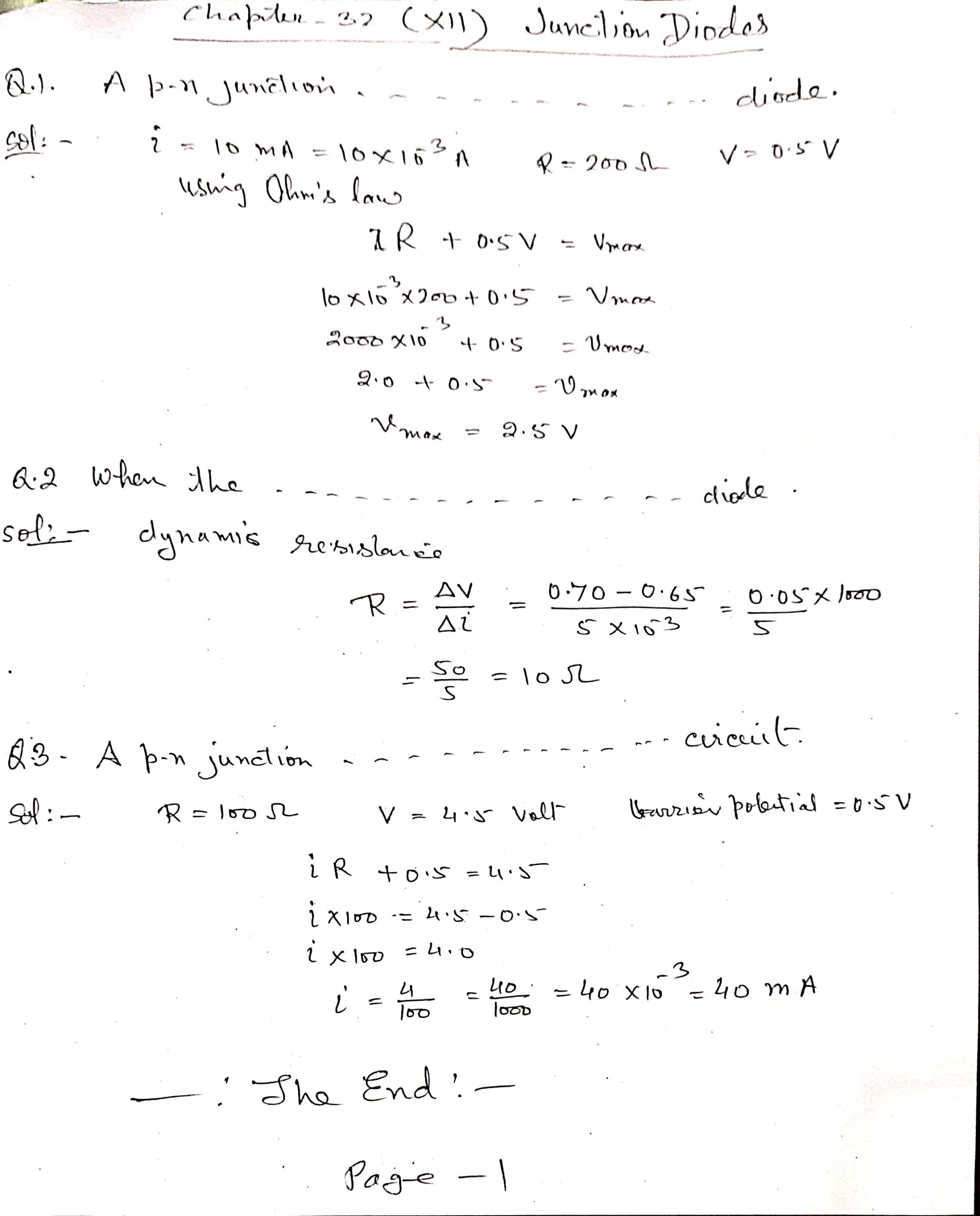
Question 1:
A p-n junction diode can withstand currents up to a maximum of 10 mA. A resistor ………………….. forward bias the diode.
Question 2:
When the voltage drop across a p-n junction from ………………………. of the diode?
Question 3:
A p-n junction diode is connected to a series resistor …………………….. find the current in the circuit.
—: End of Nootan Solutions Junction Diode :–
CONTACT FOR LIVE CLASSES -9335725646
Return to – Nootan Solutions for ISC Physics Class-12 Nageen Prakashan
Thanks